|
Product Description:
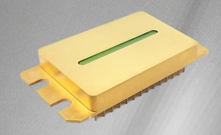
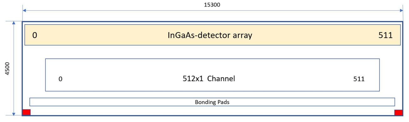
Precision Micro-Optics offers cooled near-infrared linear image sensor consisting of a linear InGaAs-detector array bonded to the p-on-n readout IC.
Product Features:
- 512X1 Pixels (25X250um or 25X500um)
- 28-pin Metal DIP Package
- Embedded Thermoelectric Cooler
- Built-in Temperature Sensor
- 0.9 μm – 1.7 μm Spectral Range
- Minimum Pixel Operability > 99%
- Quantum Efficiency > 70%
- Snapshot ITR / IWR
- 2 Outputs with up to 22 MHz Pixel Rate
Applications:
- Shortwave-Infrared Imaging
- Semiconductor Inspection / Process Monitoring
- Near-Infrared Spectrophotometr
SPECIFICATIONS (ITS = 20 ± 1ºC)(Readings from Integrated Temperature Sensor (ITS)):
Parameters
|
Symbol
|
Test conditions
|
Min
|
Typ |
Max
|
Unit |
Sensor Technology
|
|
|
Planar InGaAs PIN
|
|
Actual Pixel Array
|
|
|
512 x 1
|
|
Pixel Pitch
|
|
|
25
|
um
|
Pixel Size (S)
|
|
|
25 X250
|
um
|
Pixel Size (M)
|
|
|
25 X500
|
um
|
Spectral Response Range
|
λ
|
|
900
|
|
1700
|
nm
|
Dark Current (S)(*)
|
ID
|
VR = 0.5V
|
|
|
0.6
|
nA
|
Dark Current (M)(*)
|
ID
|
VR = 0.5V
|
|
|
1
|
nA
|
Quantum Efficiency * Fill Factor(*)
|
QEFF
|
λ = 1550nm
|
70 |
|
|
%
|
Response Nonuniformity(*)
|
|
At 50 % Full Well
|
|
|
5
|
%
|
Response Nonlinearity
|
|
15 % – 85 % Well Occupation Range
|
|
|
2
|
%
|
Charge Capacity
(16 settings)
|
|
Cint = 6.4 fF
|
|
25
|
|
μV/e-
|
Cint = 16 fF
|
|
10
|
|
Cint = 30 fF
|
|
5.3
|
|
Cint = 120 fF
|
|
1.3
|
|
Cint = 2.1 pF
|
|
0.076
|
|
Readout Noise
(ROIC Specifications )
|
|
Cint = 6.4 fF
|
|
1.2
|
|
mV
|
Cint = 16 fF
|
|
0.8
|
|
Cint = 30 fF
|
|
0.6
|
|
Cint = 120 fF
|
|
0.5
|
|
Cint = 2.1 pF
|
|
0.25
|
|
Output Swing
|
|
Gain @ 120 fF
|
2.0
|
|
|
V
|
Minimum Integration Period
|
|
ROIC Specifications |
5 |
|
|
μs
|
Maximum Pixel Rate
|
|
ROIC Specifications |
|
|
22
|
MHz
|
Pixel Operability(*)
|
VBD
|
Percentage of Pixels with QEFF
Deviation ± 20%*(QEFF Mean) |
99
|
|
|
%
|
Chip Size
|
|
|
15.3 x 4.5
|
mm
|
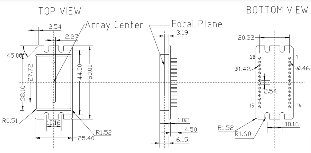
Package Type
|
|
|
28-pin Metal DIP Package
|
|
Package Size L x W x T
|
|
|
50.00 x 25.40 x 11.67
|
mm
|
Weight
|
|
|
25.8
|
g
|
Note (*): These items are defined for central effective pixel array (512x1). Their values correspond to default operation conditions.
Absolute Maximum Ratings (T=25ºC):
| |
Parameters
|
Min
|
Typ |
Max
|
Unit |
| |
Operating Temperature
|
-40
|
|
70
|
°C
|
| |
Storage Temperature
|
-40
|
|
70
|
°C
|
| |
Power Consumption
|
|
|
95
|
mW
|
Package Dimensions (mm) and Pin Definition:
| |
01
|
VDD
|
08
|
SDOUT |
15
|
GND
|
22
|
NC |
| |
02
|
RESET
|
09
|
DATVALID |
16
|
NC
|
23
|
NC |
| |
03
|
TEC+
|
10
|
VOUT |
17
|
VOFFSET
|
24
|
NC |
| |
04
|
INT
|
11
|
VDDA |
18
|
VTEMP
|
25
|
NC |
| |
05
|
MC
|
12
|
VR2 |
19
|
NC
|
26
|
TEC- |
| |
06
|
CEB
|
13
|
VR1 |
20
|
NC
|
27
|
NC |
| |
07
|
SDIN
|
14
|
VDETCOM |
21
|
NC
|
28
|
NC |
CHIP LAYOUT:
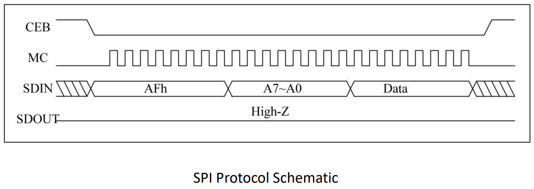
SPI Interface:
The Linear Image Sensor supports SPI protocol to set the command registers. There are functions of the gain mode,
power consumption control and the sequence of pixel output.
Bias Input :
| |
Pin #
|
Bias
|
Voltage |
Current
|
Remark |
| |
01
|
VDD
|
1.8 V |
> 30 mA
|
Positive logic supply
|
| |
11
|
VDDA
|
3.6 V |
> 60 mA
|
Positive analog supply
|
| |
12
|
VR2
|
0.3 V |
> 30 mA
|
External Input Bias
|
| |
13
|
VR1
|
2.3 V |
> 5 mA
|
External Input Bias
|
| |
14
|
VDETCOM
|
> VR1 |
|
Detector common voltage
Detector bias = VDETCOM - VR1 (*)
|
| |
15
|
GND
|
0V |
|
Ground
|
| |
03
|
TEC+
|
0 V ~ 5.3 V |
< 2.2 A
|
Positive TEC supply
|
| |
26
|
TEC-
|
0 V |
|
TEC ground
|
| |
02
|
RESET
|
1.8 V |
|
Chip reset
|
| |
17
|
VOFFSET
|
0.3 ~ 2.3 V |
> 30 mA
|
Offset Input Bias
|
Note (*): VDETCOM lower than 2.3 V will forward bias the sensor, the exact zero bias voltage is device and temperature dependent.
Digital Pattern Input :
| |
Pin #
|
Clocks
|
Levels |
Rise/Fall
|
Remark |
| |
04
|
INT
|
1.8 V / 0 V |
< 50 nS
|
Integration time
|
| |
05
|
MC
|
1.8 V / 0 V |
< 5 nS
|
Master clock,
Max. Freq. = 22 MHz
|
| |
06, 23
|
CEB
|
1.8 V / 0 V |
< 10 nS
|
Chip enable(*)
|
| |
07
|
SDIN
|
1.8 V / 0 V |
< 5 nS
|
Data code input
|
Note (*): The input and output of all commands start after the falling edge of CEB.
Digital Pattern Output :
| |
Pin #
|
Clocks
|
Levels |
Rise/Fall
|
Remark |
| |
08
|
SDOUT
|
1.8 V / 0 V |
|
Data code output
|
| |
09
|
DATVALID
|
1.8 V / 0 V |
|
Valid data output flag signal
|
Analog Output :
| |
Pin #
|
Outputs
|
Levels |
Value
|
Remark |
| |
10
|
VOUT
|
0.2 ~ 2.4 V |
|
Video output
|
| |
18
|
VTEMP
|
2.138 V |
27℃
|
Integrated Temperature Sensor (-0.6 mV /℃)
|
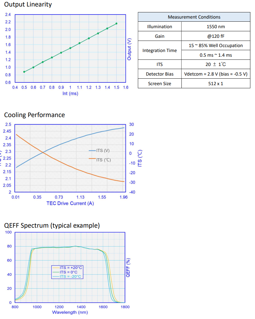
Figures :
|